Advancing Semiconductor Innovation: Imec's Roadmap for the Future of Transistors
Imec has released its semiconductor process technology roadmap, which not only outlines critical developments expected over the next few decades but also highlights the challenges the industry will confront. Collaborating with tech giants like TSMC, Intel, and Nvidia, Imec anticipates a future where traditional scaling mechanisms evolve into new transistor technologies.
Central to this roadmap is the ambitious goal of achieving 3 angstrom-class (0.3nm) fabrication technologies by 2038. However, Imec predicts a halt in the shrinking of contact poly pitch (CPP) by 2030, suggesting that the classic principles of Moore's Law may need recalibration. To maintain progress in chip density, the incorporation of advanced technologies such as CFET transistors and High-NA EUV lithography systems appears essential.
GAA Transistors and Their Road Ahead
The complexity of semiconductor manufacturing has shifted from introducing entirely new process technologies every couple of years to launching new node generations approximately every three years, supplemented by yearly enhancements. TSMC, for instance, has rolled out N3B in 2023, with plans for N3E in 2024 and N3P in 2025. Meanwhile, Intel initially planned launches for 20A in 2024 and the 18A node in 2025, albeit with delays.
This gradual progression in process technology is echoed in Imec's roadmap. Its journey into the 2nm-class era (N2) showcases a CPP of about 48nm, alongside a cell height of near 132nm with six metal tracks. This leads to a natural question about Intel’s and TSMC’s respective advancements, with Intel’s 18A featuring a CPP of 50nm and varying cell dimensions for density and performance.
Julien Ryckaert, Imec’s Vice President of R&D, has indicated that beyond the 2nm threshold, we will encounter a transformative phase into Angstrom nodes, as Imec’s logic roadmap extends beyond N2.
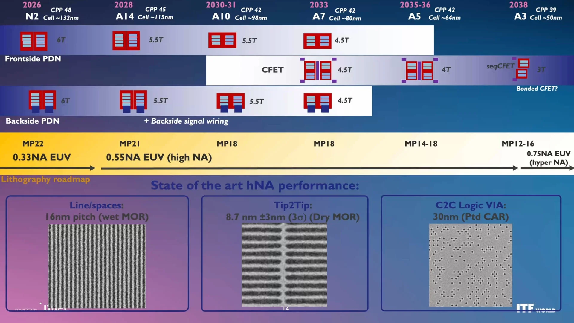
The forthcoming A14-class technology is anticipated by 2028, with TSMC expected to begin high-volume production soon after. This node promises a CPP reduction to 45nm and a cell height of 115nm, alongside a decrease in metal tracks to 5.5. Looking beyond the immediate horizon, Imec envisions an A10-class technology around 2030, which will settle at a CPP of 42nm.
Interestingly, the implementation of gate-all-around (GAA) transistor nodes is projected to adapt to various power delivery network designs, suggesting that while back-side power delivery is a future goal, it won’t immediately apply across all uses.
The Rise of CFET Technology
Perhaps the most engaging part of the roadmap is its focus on CFET technology. Slated for potential deployment during the A7 generation in 2033, CFET differentiates itself by stacking n-type and p-type transistors vertically. This approach enhances transistor scaling and positions CFET as a leading player in future processes.
As conventional nanosheet architectures near their practical limits, Imec sees CFET stepping in at A7, though adoption might be variable due to a consistent CPP at 42nm. Notably, the use of back-side power delivery networks appears to be integral for making the most out of CFET designs. Ryckaert has emphasized the scaling challenges faced in the pursuit of more effective semiconductor architectures.
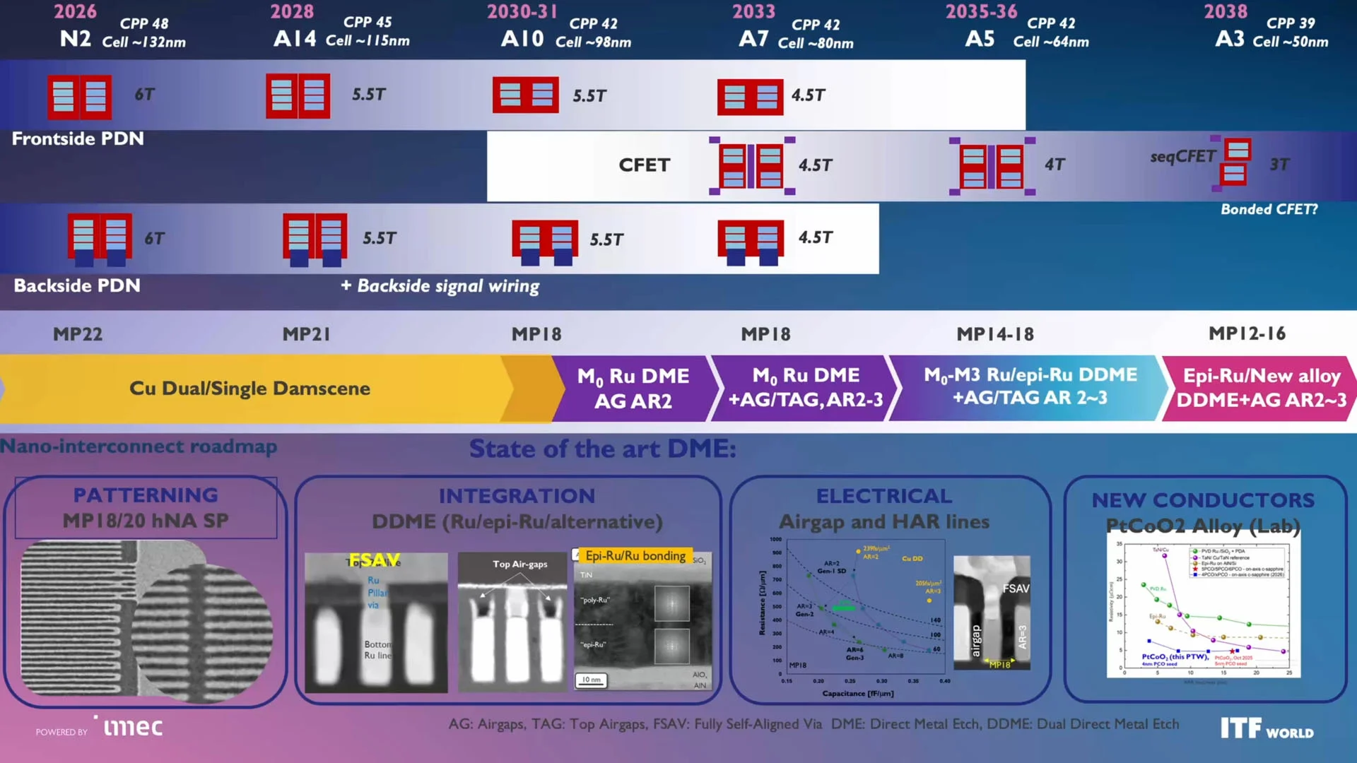
By the time we reach the A5 generation around 2035-2036, efficiencies will continue to emerge, with a reduction in cell height to around 64nm through a 4-track library. By 2038, A3 technology levels will demand even finer control with a 39nm CPP and a target cell height of 50nm, necessitating the use of advanced lithography techniques.
Rethinking Moore's Law
Imec's roadmap effectively reinterprets the implications of Moore's Law. Traditionally viewed as an ongoing increase in transistor counts on a chip, it now appears that gains in density must pivot towards new design paradigms. The roadmap indicates a stagnation in CPP from A10 through A5, suggesting that developers will increasingly focus on how to fit more logic gates into existing structures—and less on reducing the size of transistors.
This shift means metrics such as the size of standard cell libraries will take precedence over merely assessing the dimensions of individual transistors. With companies designing chips around blocks built from standard cells, a more complex understanding of logic density will emerge. The transition expected from six-track designs at N2 to three-track architectures at A3 exemplifies how future density improvements depend on enhancements in standard cell dimensions.
Heterogeneous Integration and Co-Optimization
The semiconductor sector is on the cusp of what Imec terms Heterogeneous Large-Scale Integration (HLSI). This new paradigm highlights a shift away from solely enhancing transistor density towards the integration of diverse technologies in unified platforms. For successful deployment of future AI-driven architectures, combining logic, memory, and optical I/O technologies will be paramount.
Imec’s Cross-Technology Co-Optimization (XTCO) framework is set to assess the interactions between various system components, focusing on optimizing system efficiency overall. However, the challenge remains that the development of individual technologies—like logic at foundries and cooling solutions by external vendors—might complicate coherent advancements in this new directive.
Navigating Power and Cooling Challenges
As chip density escalates, power distribution is set to become a major bottleneck. Leading manufacturers, including Intel and TSMC, are already implementing backside power delivery technologies to enhance power efficiency, while future designs will likely incorporate advanced voltage regulation techniques. The cooling of these increasingly power-hungry setups will be equally critical, demanding innovative thermal management strategies.
Imec’s projections insist on integrating sophisticated cooling and thermal optimization techniques alongside future chip designs. As the industry prepares for multi-chiplet packages, the requisite developments for effective thermal management become imperative, as Ryckaert notes: addressing energy costs related to data movement and enhancing thermal dynamics is non-negotiable.
Charting the Future of Semiconductor Technology
Imec's thorough roadmap extends into the foreseeable future of semiconductor innovation, positing that Moore's Law can persist despite diminishing rates of traditional transistor scaling. The anticipated transitions between GAA, CFET, and advances in vertical integration signal a pivotal transformation in how transistor density can be achieved going forward.
As the industry stands on the verge of what could be a fundamental transformation in semiconductor design philosophy, the challenge will be more than just manufacturing smaller transistors; it will hinge on effectively delivering power and managing heat for enhanced performance.